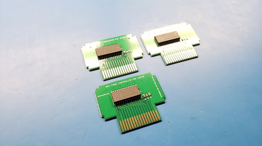
Ever had your N64 memory pak battery die and lose all your precious saves from your childhood games? Or purchase an aftermarket pak only for it to arrive broken? I have, which is why I designed my own N64 memory pak. I used an FM28V020 FRAM IC which does not require a battery to retain the saves and according to the datasheet it will last 150 years! Most FRAM modded paks I see use parts harvested from an original nintendo memory pak so instead I designed my own pcb so I can build the whole device with off-shelf purchased parts.
The pcb will even fit perfectly in an original nintendo memory pak shell in that case that you want to swap them. I modeled the memory pak shell to be 3D printed.
The memory size is 256KB, which is the same size as the original pak. Due to the memory bank size, it is not possible to use a larger memory. Some aftermarket paks that advertise extra memory, quite literally have two memory ICs inside with a switch to activate either chip.
I think this has turned out to be a good product that is needed in the market flooded with over priced FRAM modded paks so I will be selling them on ebay. Get yourself a reliable memory pak that will keep its saves for generations!
The record to build the world’s smallest N64 portable gripped my imagination since I was a young teenager just getting into portablizing. Each new record pushed the N64 motherboard to its limit of trimming advancements and case layout imagination. I’m proud to finally hold the record after all these years!
The trim I used is based on the Advanced N64 trim from the new Advanced N64 Trimming guide on Bitbuilt.
I cut it even smaller as close as possible to the required components. I trimmed off the cartridge connector and rewired the signals back to the RCP/CPU. Then I desoldered the RAM expansion slot and resoldered it at 90 degrees to make it as thin as possible. The motherboard could still be trimmed smaller however it would require rewiring many more sub-circuits and no space is gained as the limiting factor here is the cartridge and the 3.5″ screen. Using a cartridge emulator like the 64drive/ed64 would not help to make it smaller because the cartridge slot has smaller volume than increasing the thickness of the device with the new pcb.
Using a 1st party N64 controller and 2 microcontrollers for interfacing the Joycon joysticks. Pressing the left stick click is the N64 L button. Pressing the right stick click changes the left stick between analog and dpad mode. Sacrifices had to be made to fit it in such a small enclosure. The final volume is 270,863.87 millimeters cubed!
Oh yeah and the best part is that since I didn’t have any more N64 motherboards on hand to use, I ripped an N64 motherboard out of a broken Millsdj portable someone sent me and trimmed it again (the holder for the previous record).
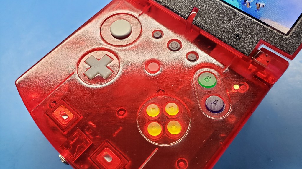
The N64SP has made a come back and now with funtastic cases! I feel like this is something I’ve wanted to make since the beginning and finally funtastic cases are achievable.
The case is made by printing it in clear resin on a Form2 3D printer. After sanding it up to 1,000 grit, I painted it with Tamiya TS series clear paint. I’ve had the Form2 for about 2 years now but haven’t really used it much until now. I’m so glad I hung onto it.
The PCB now uses a real N64 controller IC with an FRAM chip for saving games. The battery management, system regulators, audio amp, and controller are all combined in one 2layer PCB.
The buttons were also printed on the Form2, then casted, and molded in dyed resin. This is an easier process as it is more repeatable rather then printing the buttons and painting them.
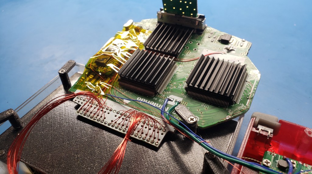
The trim features the PIF relocation which makes the board a good deal smaller. I used a custom PIF breakout PCB to facilitate the relocation. I plan to consolidate this all into a guide soon. I also swapped the 2 2MB RAM chips with 2 4MB chips for double the memory without the added size of the expansion pak. This build has pretty much everything you could ask for besides controller/video out which I still stand by is kind of gimmicky for these devices.
And would you look at that? An actual heatsink this time! Way to go!
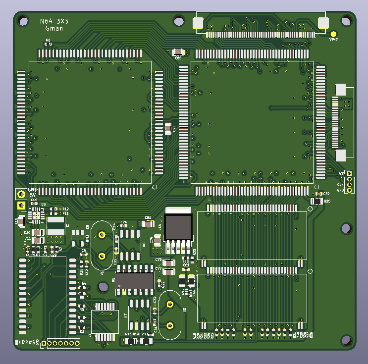
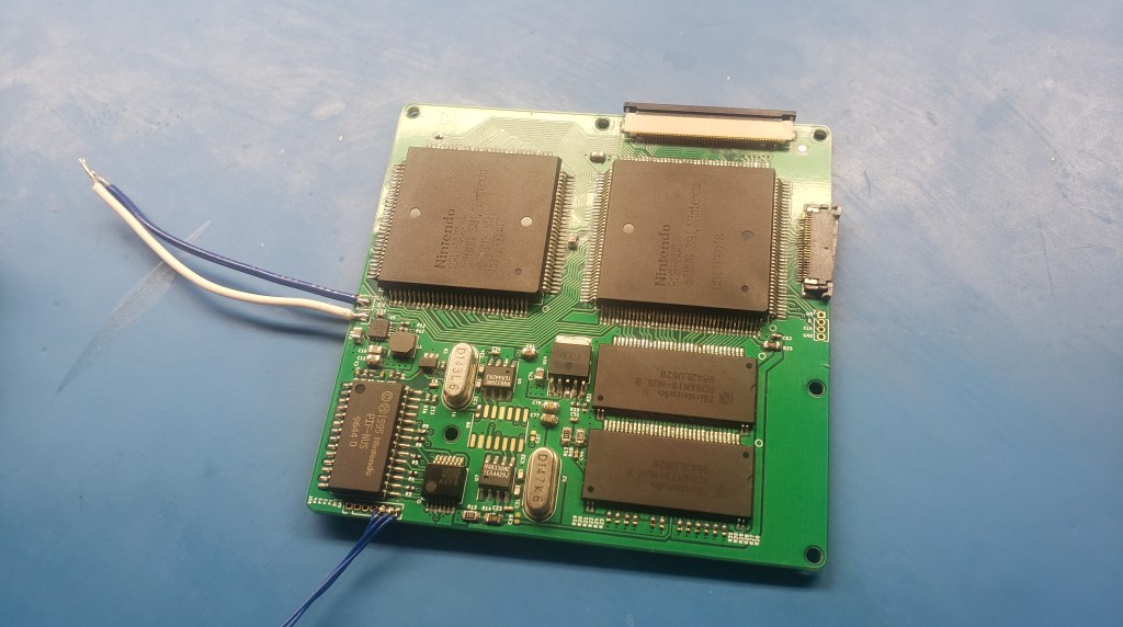
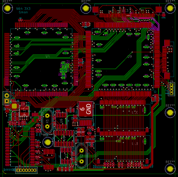
The N64 3X3 is a redesigned N64 circuit 3 inches on each side. About 2 years ago for a fun summer project I mapped out the whole N64 schematic, I made a layout but stopped there from lack of pcb design confidence. With the excitement on my N64 projects recently I revisited the project after realizing the more you trim off the N64, the more relevant a new pcb would be. I looked over the original schematic I made and there was a few things missing and redid the layout.
First I’ll start by giving credit where credit is due, the first N64 3X3 was made by Marshallh however the project had been halted in favor of other things so I decided to pick it up and run with it as far as I can and hopefully we’ll see it into a portable. Also I have to thank him for helping me debug the pcb.
The trickiest part of the layout certainly being the RDRAM routing, I kept the traces straight with ground in between and the termination resistors as close as possible and crossed my fingers.
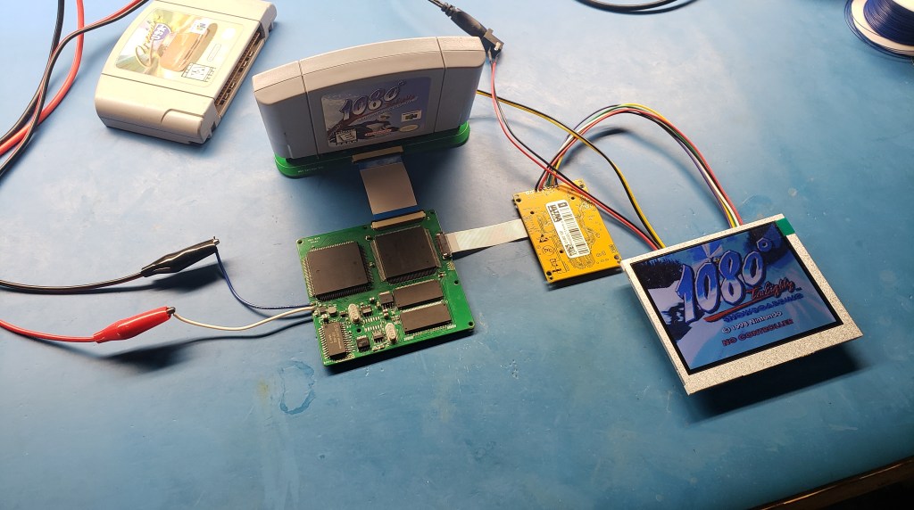
At the top of the PCB is a 50pin FFC connection for the cartridge and on the right is a 26pin connection for digital video output. I designed it to interface with the ultraVGA/HDMI mod. It uses an FPGA to create high quality video output. There are 2 variations of the stock N64 video circuit which could complicate the PCB and I think most people nowadays are only interested in VGA anyway so that was my choice. Audio output will be only through custom digital audio amplifier too.
This is just the beginning for this project. I’ve confirmed my schematic and asset is correct and working and now I can add more to it to be used in a complete gaming system. My hope is to make some variation of it opensource for anyone who wants to make a compact and neat N64 portable. I enjoyed the most learning deeper into the N64 hardware and mapping out the minimum required components for the circuit which helped tremendously for trimming too.
Funny how I must be the last person to write an article on my own device! The N64 SP is finished, and I absolutely love it.
I made an all-in-one PCB which includes the N64 power regulators, battery management, USBC PD charging capabilities, a digital N64 audio amp (from the previous article), and an N64 controller emulator (being developed by my friend Aurelio, he let me try it out). On the back side of the PCB are all the controller buttons and a connection for the 3DS joystick. This board really eliminates so many wires in the device.
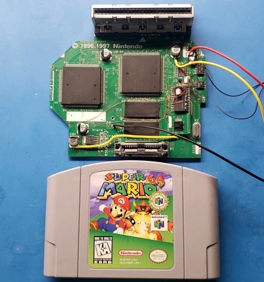
This is my favorite N64 cartridge slot in a portable. I get a lot of criticism about how the device is too thick. It’s not wrong, but half the thickness is the cartridge and being able to use real n64 cartridges is a fundamental part of my idea.
A few years ago I hoarded several ultraVGA modchips from a limited time buy. I am finally able to use my first! The modchip turns the digital video from the n64 into super crisp VGA, it looks fabulous. With the digital audio and VGA used, this is one of the highest fidelity N64 experiences. This also means that the N64 on-board audio/video encoder is 100% bypassed, I am not even supplying power to it on my trimmed board.
The case is fdm printed on my Prusa MK3. I think I will recase the electronics in a better case printed on my Form2 soon. Consider this unit like a first functional prototype, I’ve already made some edits to the model taking what I learned after building it.
The N64 used to be the most popular system to portablize, we’d see a new N64p almost every week. Then as we pushed onto modern systems, the N64 saw less and less action. The N64 was basic enough to cut down, but was notoriously finicky when doing ambitious trims and would sometimes stop working for seemingly no reason. For a console that was portablized since the beginning of this hobby, it was the least well documented and we knew very little about its inner connections.
Modders have pondered for years if it were possible to do a PIF relocation since the motherboard is known for requiring specific trace impedances and doing a wire relocation might not be physically possible. I decided to give it a try to put the myth to rest. First I cut off the section of the board with the PIF on it. Then using the N64 rev9 motherboard compendium provided from my pal ShockSlayer, I traced out the connections and recreated everything with wires.
Fig 1. N64 rev9 Motherboard Compendium
To my surprise, it actually worked!! By going through the motions, I learned a lot about the N64 too. From referencing the compendium as well as trial and error I determined the required components needed for relocation and the components that could be removed. For example, the 4 controller data line pull up resistors were all required for the console to boot along with several other pull-ups. I believe this was the reason that made the N64 so notorious to stop working, turns out we’d just been doing it wrong for years. Noah and I will be working on a modern N64 trimming guide to include the PIF relocation which we hope will be very straightforward and the only way you won’t be able to get it to work is if you short 3.3v->GND. No more guesswork and finicky uncertainty.
Fig 2. 2020 N64 Trim like no other
With the U-AMP, I’ve got digital audio working with the PS2, Wii, and Dreamcast. N64 will be the next to conquer. The N64 I2S is a little strange because the audio sampling frequency can be set arbitrarily by the game and it can even change mid game! Another obstacle is that the N64 doesn’t have an I2S master clock. Using an I2S DAC would be difficult because every time the sampling frequency changes, the audio config will need to be changed as well otherwise it won’t work. A dynamic solution is required. What I ended up rigging together was a U-AMP along with a PLL IC to generate the master clock signal referenced from the I2S word select. I chose a multiplication of 512 x WS which I calculate should give a minimum compatible sampling frequency of around 12K Hz, this should be plenty of headroom for the N64.
Fig 3. U-AMP with PLL IC spaghetti wired. This will allow me to remove the MAV-NUS (audio + video dac).
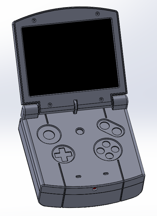
With these two major advancements, I’ve started a new N64 portable to showcase what is now possible. I always thought it would look great to make an N64P with an enclosed cartridge slot, rather than sticking far out like most.
Fig 4. My N64 portable concept design. I will share more information on it soon as progress is made.
It’s now 2020, I don’t see myself using normal old analog audio in a portable ever again. I’ve got digital audio working for PS2, Wii, Dreamcast, and even almost N64. Digital audio has the benefits of being able to bypass the digital-to-analog audio converter present on motherboards which takes out the middle man to reduce interference on the audio output. This also gives the best audio quality you can have in a portable and allows us to trim motherboards smaller in some cases.
The portablizing community has needed a good audio solution for a very long time. The only audio amps commercially available are portable speakers, which is a bad hack. And the PAM8803, which doesnt have a headphone amplifier. Neither of these solutions is ideal.
Using what I learned getting digital audio working on each systems, I set out on a new project I would call “U-AMP” (Universal-Amp). This would be ONE pcb which has the features of seamlessly integrated speakers and headphones with a variety of input sources for digital audio from Wii, PS2, Dreamcast, as well as analog audio input. It does it all. The board is based around the LM49450 IC which I have used many times. The amp is controlled by a PICLF15324; the LF version of the same PIC I use in the WiiPMS. I added two jumpers on the pcb which set the audio configuration between the four input sources. The code will configure the LM49450 to operate in the correct console mode. It also handles volume control. I added the feature to be able to hold the volume plus/down and it will periodically increase, rather than tapping it fiercely. It also has a quick mute feature by pressing the plus and minus buttons at the same time to toggle mute.
The U-AMP is now available for purchase in the BitBuilt store and fully opensource on my github
About a year ago I started on my analog polysynth project. I made progress with the initial analog sound engine design but then pushed the project on the back burner. I’m back in the groove now after gaining some more experience with microcontrollers this past year.
I’m tempted to use PIC32 for the project since I am most comfortable with it, however I will use the opportunity to learn a new 32bit platform: STM32. It’s probably for the best not to use PIC32 for this project because PIC32 communication peripherals silicon errata notoriously do not always function at higher speeds.
I have chosen an STM32F446 as the voice card mcu mostly because it has two SAI modules (Serial Audio Interface) which are capable of outputting 4 I2S TDM streams (Inter-IC Sound Time Division Multiplexing) for the possibility of 32 24bit DAC channels. The reason for 24bits of precision is the ability to eliminate the exponential conversion analog circuitry for the oscillators. Instead, the exponential conversion can be done in software and using linear oscillators which will have better tuning stability. Most of the legendary polysynths will use exponential VCOs with inherent tune drifting which is a large part of the vintage tone many people are after. But from an engineering standpoint, linear oscillators are a far better design.
An 8 channel I2S 24bit DAC is chosen for high number of outputs, high precision, and competitive price of $3.02 per IC. Each voice will need around 16 outputs meaning each mcu can control 2 voices, this will save money on the bill of materials as a polysynth needs several voices.
STM32 is mostly uncharted territory for me so I’m taking the project in small steps. First I designed the DAC control board with the STM32 and 4 I2S DACs to asses the components and verify the digital framework before wasting money on larger prototypes that might never be able to work. The next step will be to design the analog board to interface with the control board. Once the digital and analog sections are working, they will be combined into one voice card.
What will the voice card do?
The voice card is essentially an individual programmable monophonic synthesizer. Stack a few voice cards together controlled by a master CPU, and you have polyphony. The voice card will be programmed by a SPI interface that transmits all the sound engine parameters like oscillator pitch, note press triggers, filter frequency, audio mixing levels as well as parameters for the envelope generators, low frequency oscillators, and modulation routing that are all generated in software. For example, the master cpu could transmit parameters of a triangle wave at .1Hz and 10% amount applied to filter frequency. The voice card mcu will run firmware to output the modulation to the correct DAC channel. The voice card has a digital section comprised of the MCU and DACs, and an analog sound section comprised of the oscillators, filters, and voltage controlled amplifiers for controlling the software generated modulation.
There’s plenty of voice card development ahead for me. Then there is also the master CPU, user interface, and industrial case design to be done. The only way I’ll be able to finish is by tackling it one small step at a time.
The USB-C PD Charging + Internal USB Drive: This pcb gives your portable the power of USB-C Power Delivery charging and the ability to transfer files to your portable all through the USB-C port. It’s an awesome feature that makes your portable one step closer to an official device. This board was specifically developed for the WiiBoy rev3 but now it is available for purchase for anyone to share in the greatness of USB-C. https://store.bitbuilt.net/usb-c-pd-charging-internal-usb-drive/
It is slightly revised from my original design to be a little smaller and even has an integrated button which can be used for the portable’s power button.
N64PMS brings the assets of the WiiPMS circuit: 3.3v and 5v custom regulators, battery charging with dynamic play/charge, and a push button with RGB led interface to the N64. The N64 is one of the oldest consoles we’ve portablized but for over a decade it has only been done using the PTH08080 regulators. This board can bring the N64 portables into the modern age of portablizing. https://store.bitbuilt.net/n64-power-management-system/
September was a huge month for the Bitbuilt store and we’ve got even bigger things planned for October.
The Sega Dreamcast uses a proprietary digital protocol called the “Maple Bus”. It is a unique two-wire bi-directional signal where each data line alternates between taking the task of data and clock every other bit — woah.
When using common protocols like UART, I2C, SPI, etc these protocols are handled in hardware circuitry built inside the microcontrollers usually. Then the C code simply refers to the transmit / receive buffers along with the flags. This is ideal since the code does not have to be stalled during transmission and can focus on more pressing tasks.
However, the Maple bus is proprietary so you won’t find any microcontroller with a hardware Maple peripheral. You could use an FPGA, but I chose to use a microcontroller instead. Thus bit banging is required, where the protocol is implemented in software.
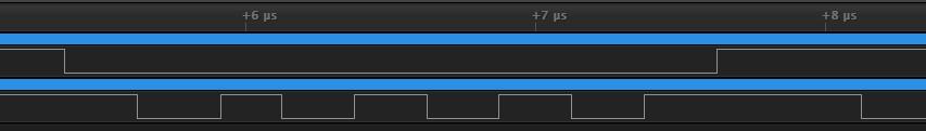
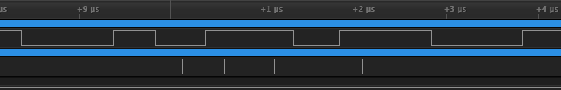
A Maple transmission is begun by a starting sequence to initiate the transmission. Both data lines start at the high position, data 1 is pulled low and remains low. Then data 2 is pulsed 4 times and holds high. Then data 1 goes high and data 2 is pulled low again. Data 1 is high and data 2 is low, this is how each 2-bit phase begins.
Here is the starting sequence captured by a logic analyzer.
A byte is transmitted in 4 2-bit phases. Phase 1: Data 1 is high, data 2 is low. Data 2 transitions to the level of the bit to be transmitted. Data 1 then pulls low and the bit is clocked in. Then data 1 transitions to the next bit and data 2 is pulled low, clocking in the bit. The phase is complete and it starts over again. Since data is always clocked in on the opposite data line of a falling edge, we really don’t need to keep track of the phases after the starting sequence, we just need to look for the falling edges.
Example: “0b00011100”.
Since data is transmitted at 1MB/S, I will need to choose a fast microcontroller that will be able to accurately sample the bits. I went with the PIC32MZ as I had some prior experience with that microcontroller for another project. The PIC32 can have a maximum CPU clock of 200MHz, estimating that an instruction can be executed on each clock (which isn’t always true), then I will be left with 200 instructions to sample each bit — even with my poor amateur code, it should be do-able!
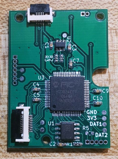
The custom controller PCB I designed with the PIC32 and some additional hardware to be used later for the VMU emulation like the FRAM chip and OLED screen.
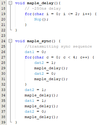
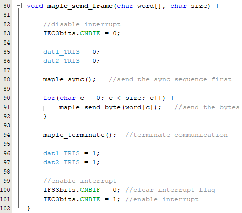
First I implement the transmitting code.
The maple_delay() function will be used for timing throughout the rest of the code. This is pretty easy so far, setting the data lines high and low to match the original controller.
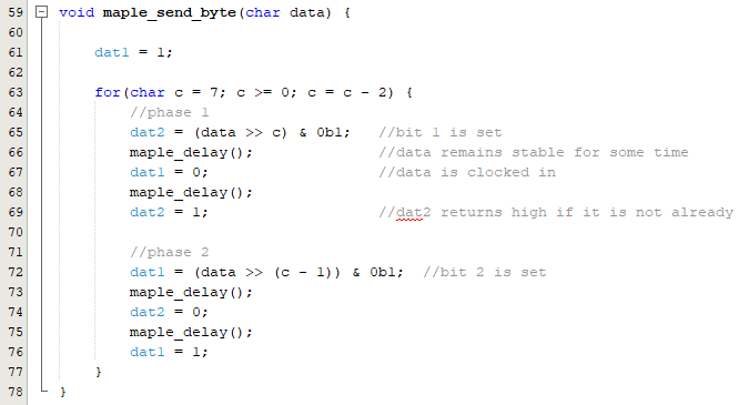
Sending one byte of data meticulously through the phases.
Finally the basic bit functions can be sorted together to send an entire word (4 bytes)!
With the transmitting done and out of the way, time to figure out how the heck I will handle receiving bits. I can’t just sample the data lines forever in a loop because the microcontroller needs to handle other tasks like sampling the controller buttons, joystick ADC, and formulating the response packet.
After trying several methods out, the way it worked reliably enough was to capture the starting sequence using an interrupt flagged from the falling edges of the data lines. When the starting sequence is matched to be true, it disables the interrupt and samples the bits in a loop until the entire word is received. I’m not too happy about this method because it is limiting and the CPU is stalled during the entire receiving transmission. It is also very memory hungry, needing to sample each falling edge and then package the data into the bytes they belong afterwards. But I digress, it works reliably enough for a playable controller. There’s nothing ideal or perfect about bit banging a protocol in software anyway.
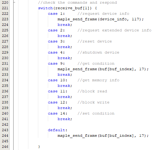
With the protocol implemented, the controller commands can be sampled and responded with the correct packet response. I only have two commands implemented for basic functionality controller. The other commands are for VMU which is currently not implemented at all, I will need a more robust receiving protocol before I tackle that since many more words will need to be accurately sampled one after another.
The software has a ways to go, but I’m pleased that I was able to get it working this far. I certainly learned a lot through this project.